- 您现在的位置:买卖IC网 > Sheet目录3822 > PIC18F4525-I/ML (Microchip Technology)IC MCU FLASH 24KX16 44QFN
PIC17C4X
DS30412C-page 158
1996 Microchip Technology Inc.
Applicable Devices 42 R42 42A 43 R43 44
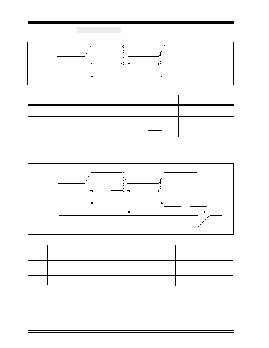
FIGURE 17-5: TIMER0 CLOCK TIMINGS
TABLE 17-5:
TIMER0 CLOCK REQUIREMENTS
FIGURE 17-6: TIMER1, TIMER2, AND TIMER3 CLOCK TIMINGS
TABLE 17-6:
TIMER1, TIMER2, AND TIMER3 CLOCK REQUIREMENTS
Parameter
No.
Sym Characteristic
Min
Typ Max Units Conditions
40
Tt0H T0CKI High Pulse Width
No Prescaler
0.5TCY + 20 §
—
ns
With Prescaler
10*
—
ns
41
Tt0L T0CKI Low Pulse Width
No Prescaler
0.5TCY + 20 §
—
ns
With Prescaler
10*
—
ns
42
Tt0P T0CKI Period
TCY + 40 §
N
—
ns
N = prescale value
(1, 2, 4, ..., 256)
*
These parameters are characterized but not tested.
Data in "Typ" column is at 5V, 25C unless otherwise stated. These parameters are for design guidance only and are not
tested.
§
This specication ensured by design.
Parameter
No.
Sym
Characteristic
Min
Typ
Max
Units Conditions
45
Tt123H
TCLK12 and TCLK3 high time
0.5 TCY + 20 §
—
ns
46
Tt123L
TCLK12 and TCLK3 low time
0.5 TCY + 20 §
—
ns
47
Tt123P
TCLK12 and TCLK3 input period
TCY + 40 §
N
—
ns
N = prescale value
(1, 2, 4, 8)
48
TckE2tmrI Delay from selected External Clock Edge to
Timer increment
2TOSC §
—
6 Tosc §
—
*
These parameters are characterized but not tested.
Data in "Typ" column is at 5V, 25C unless otherwise stated. These parameters are for design guidance only and are not
tested.
§
This specication ensured by design.
RA1/T0CKI
40
41
42
TCLK12
45
46
or
TCLK3
TMRx
48
47
发布紧急采购,3分钟左右您将得到回复。
相关PDF资料
DSPIC30F2023-30I/ML
IC DSPIC MCU/DSP 12K 44QFN
PIC16LF767-I/ML
IC PIC MCU FLASH 8KX14 28QFN
PIC18LF2320-I/SO
IC MCU FLASH 4KX16 EEPROM 28SOIC
PIC18F4458-I/ML
IC PIC MCU FLASH 12KX16 44QFN
DSPIC33FJ64GP706A-I/PT
IC DSPIC MCU/DSP 64K 64-TQFP
PIC16F874-20/P
IC MCU FLASH 4KX14 EE 40DIP
DSPIC33FJ64GP706-I/PT
IC DSPIC MCU/DSP 64K 64TQFP
PIC24HJ128GP210-I/PT
IC PIC MCU FLASH 128KB 100TQFP
相关代理商/技术参数
PIC18F4525-I/P
功能描述:8位微控制器 -MCU 48KB 3968 RAM 36I/O RoHS:否 制造商:Silicon Labs 核心:8051 处理器系列:C8051F39x 数据总线宽度:8 bit 最大时钟频率:50 MHz 程序存储器大小:16 KB 数据 RAM 大小:1 KB 片上 ADC:Yes 工作电源电压:1.8 V to 3.6 V 工作温度范围:- 40 C to + 105 C 封装 / 箱体:QFN-20 安装风格:SMD/SMT
PIC18F4525-I/P
制造商:Microchip Technology Inc 功能描述:IC 8BIT FLASH MCU 18F4525 DIP40
PIC18F4525-I/PT
功能描述:8位微控制器 -MCU 48KB 3968 RAM 36I/O RoHS:否 制造商:Silicon Labs 核心:8051 处理器系列:C8051F39x 数据总线宽度:8 bit 最大时钟频率:50 MHz 程序存储器大小:16 KB 数据 RAM 大小:1 KB 片上 ADC:Yes 工作电源电压:1.8 V to 3.6 V 工作温度范围:- 40 C to + 105 C 封装 / 箱体:QFN-20 安装风格:SMD/SMT
PIC18F4525-I/PT
制造商:Microchip Technology Inc 功能描述:IC 8BIT FLASH MCU 18F4525 TQFP44
PIC18F4525T-I/ML
功能描述:8位微控制器 -MCU 48KB 3968 RAM 36I/O RoHS:否 制造商:Silicon Labs 核心:8051 处理器系列:C8051F39x 数据总线宽度:8 bit 最大时钟频率:50 MHz 程序存储器大小:16 KB 数据 RAM 大小:1 KB 片上 ADC:Yes 工作电源电压:1.8 V to 3.6 V 工作温度范围:- 40 C to + 105 C 封装 / 箱体:QFN-20 安装风格:SMD/SMT
PIC18F4525T-I/PT
功能描述:8位微控制器 -MCU 48KB 3968 RAM 36I/O RoHS:否 制造商:Silicon Labs 核心:8051 处理器系列:C8051F39x 数据总线宽度:8 bit 最大时钟频率:50 MHz 程序存储器大小:16 KB 数据 RAM 大小:1 KB 片上 ADC:Yes 工作电源电压:1.8 V to 3.6 V 工作温度范围:- 40 C to + 105 C 封装 / 箱体:QFN-20 安装风格:SMD/SMT
PIC18F452-BL
制造商:POWERLITE SYSTEMS 功能描述:BOOTLOADER PIC18F452 FOR FLASHLAB 制造商:POWERLITE SYSTEMS 功能描述:BOOTLOADER, PIC18F452, FOR FLASHLAB 制造商:POWERLITE SYSTEMS 功能描述:BOOTLOADER, PIC18F452, FOR FLASHLAB, Silicon Manufacturer:Powerlite Systems, Cor 制造商:POWERLITE SYSTEMS 功能描述:PIC18F452 W/ BOOTLOADER, FOR FLASHLAB, Silicon Manufacturer:Powerlite Systems, Core Architecture:PIC, Core Sub-Architecture:PIC18F, Kit Contents:Board , RoHS Compliant: Yes
PIC18F452-E/L
功能描述:8位微控制器 -MCU 32KB 1536 RAM 34I/O RoHS:否 制造商:Silicon Labs 核心:8051 处理器系列:C8051F39x 数据总线宽度:8 bit 最大时钟频率:50 MHz 程序存储器大小:16 KB 数据 RAM 大小:1 KB 片上 ADC:Yes 工作电源电压:1.8 V to 3.6 V 工作温度范围:- 40 C to + 105 C 封装 / 箱体:QFN-20 安装风格:SMD/SMT